SMPS Layout Best Practices: A Guide for Electronics Hobbyists

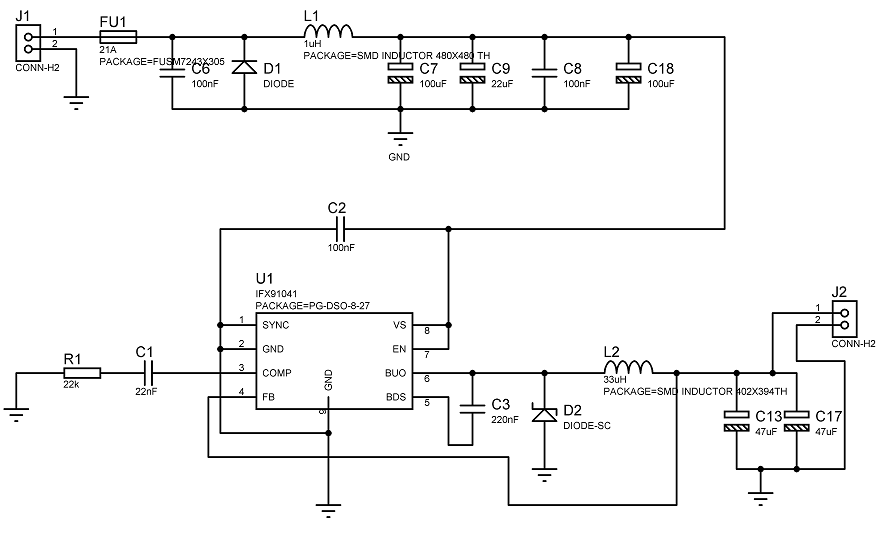
Switch-mode power supplies (SMPS) are essential for powering electronic circuits efficiently. However, designing an SMPS layout that minimizes noise and maximizes performance can be tricky, especially for hobbyists and engineers working on prototypes. The main issue often arises from improper PCB (Printed Circuit Board) layout, which can lead to inefficiencies, increased electromagnetic interference (EMI), and thermal issues.
Understanding the Issue:
In an SMPS, the layout plays a crucial role in how effectively the components interact. A poorly designed layout can cause the circuit to behave unpredictably, resulting in voltage drops, excess heat, or even component damage. The key issue to focus on is the path between the input, output, and ground. These need to be as short and direct as possible to minimize resistance and prevent unwanted noise.
Practical Example:
Imagine you’re designing a power supply for a small LED project. If the ground plane is not continuous or if the high-current paths (like the output capacitor) are too long, your circuit might experience voltage fluctuations. This could lead to LEDs flickering or the circuit overheating.
Sample Calculation:
For instance, if you’re calculating the power dissipated by a resistor, you might use the formula:
P=I2×RP = I^2 \times RP=I2×R
Where III is the current (in Amps) and RRR is the resistance (in Ohms).
For a 5V circuit with a 10Ω resistor and 0.5A current:
P=(0.5)2×10=2.5 wattsP = (0.5)^2 \times 10 = 2.5 \text{ watts}P=(0.5)2×10=2.5 watts
Make sure to use a resistor that can handle this power to avoid overheating.
Relevant Products:
For your SMPS design, consider using quality MOSFETs and capacitors for better efficiency. Shop for Made in India components at SmartXProKits.in. Support our work and India’s innovation—Shop Now our Make in India site!


