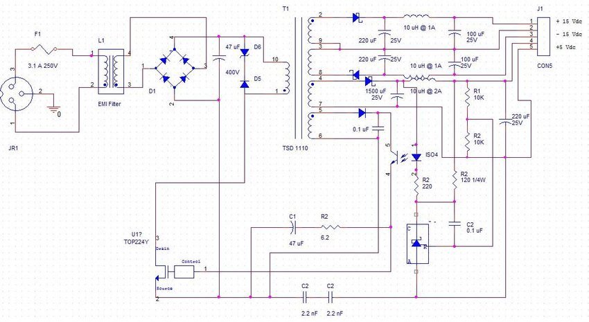
SMPS High-Efficiency Layout Tips for Prototypers

When designing a Switch Mode Power Supply (SMPS), layout is everything. Even with high-quality components, a poor PCB layout can cause overheating, EMI issues, and wasted power. Here’s how to get it right—especially if you’re a hobbyist or prototyper in India.
🔧 The Problem :
In SMPS circuits, fast switching can create noise and power losses. If your layout has long traces or poor grounding, efficiency drops fast. A clean, compact layout minimizes parasitic inductance and resistance, improving both performance and reliability.
✅The Solution :
Suppose you’re building a 5V 2A buck converter for a microcontroller. Placing the MOSFET, diode, and inductor close together reduces loop area, cutting EMI and boosting efficiency. Also, use a solid ground plane and short return paths.
🧮 Sample Calculation :
If your trace resistance is 0.05Ω and current is 2A,
Power loss = I²R = 2² × 0.05 = 0.2W.
Reducing trace resistance by better layout can cut this in half!
🛠️ Try These “Made in India” Components
Shop now at SmartXProKits.in
Support our work and India’s innovation—buy from our Make in India site!


